Learning how to solder circuit boards is not a difficult task.
Achieving proper soldering technique is something that will take practice. While learning how to solder circuit boards you will probably make a few mistakes that will require rework.
However, after a few soldering projects you will notice the improvement in your soldering skills and the progress you made.
Size of the solder joint
The size of the solder joint affects the amount of time needed for activation of flux and melting of the solder.
The bigger solder joints need more heat for solder melt to occur. Soldering irons with higher wattage should be used for bigger solder joints. In addition, a bigger solder tip should be used on soldering iron.
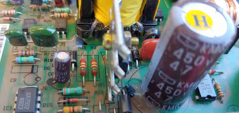
The most important thing when selecting iron’s tip is the amount of thermal linkage between the solder joint and the iron. Thermal linkage is the area of contact between solder joint and iron.
Time of soldering
After you select the right size and shape of the iron tip, you should consider the amount of time your soldering iron will be in contact with the solder joint.
The correct amount of time for soldering is between two and four seconds.
That is usually enough time for flux to activate and solder to melt and flow into the solder joint. More or less time will lead to bad soldering results. A too short time will result in cold solder joints and a too long time can result in damages to the circuit board and electronic components.
Pressure
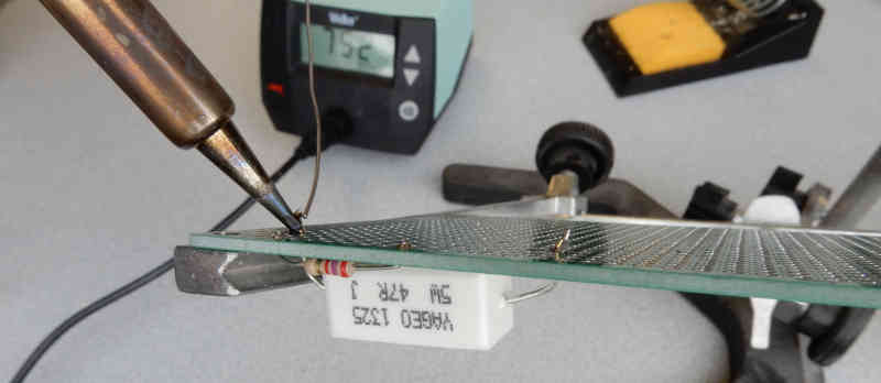
You should hold soldering iron at a 45-degree angle to the circuit board surface and apply gentle pressure. Hold it as a pen.
The level of pressure applied with soldering iron during soldering should only be enough to keep the iron in the desired place.
Too much pressure can end up with lifted and damaged pads and traces on the printed wiring assembly.
Too many times I have seen beginners in soldering strongly pushing the soldering iron to the solder joint. It happens when they use a too-small iron bit on a large solder joint and therefore they are unable to melt solder. It can also happen when they use a low-power soldering iron. They desperately try to compensate for the lack of heat by applying more pressure to the solder joint with a soldering iron. Obviously, this is a wrong soldering technique which results in damage to the circuit board.
Safety precautions
Before soldering pay attention to the following safety precautions:
Work in a well-ventilated area or use a portable bench-top fume absorber
Always keep your soldering iron in an iron stand
Don’t touch the iron tip when the iron is turned on (the iron tip is very hot)
Wear protection safety glasses
Make sure that your soldering iron never accidentally touches the body of components, chassis, wires or its power cord
Wash your hands with soap after soldering (solder contains lead)
Preparing for soldering
Soldering iron
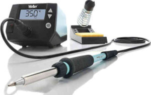
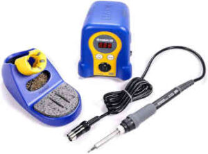
For soldering circuit boards you will need a decent temperature-controlled soldering iron. You can purchase one of those irons in the range of $ 50-$150 on the market in the USA.
These irons have a built-in setting on the base station which provides an accurate adjustment and control of temperature on the iron tip. Temperature controlled soldering iron can be used in a variety of applications on the circuit board.
We recommend using electric soldering iron when soldering electronic components on the circuit board and not an electric soldering gun. A soldering gun can be used for soldering wires, terminals and connectors but not for soldering of small or temperature-sensitive electronic components.
Selecting iron tip
You should select the size and shape of the iron tip that is most appropriate for your soldering project.
Replacement of the tip on the soldering iron should be done while the iron is cold and not plugged into the electrical power.
Iron tips are different in size and shape. It is easy to replace the iron tip on soldering iron.
Tips are interchangeable to allow the use of soldering iron in a broader range of soldering applications and to solder more different component types. This flexibility to select the shape and size of the tip allows technicians to customize soldering iron to the particular soldering project.
If the iron’s tip is too small, heating of the solder joint will take much longer than preferred. This can cause damages to circuit boards and temperature-sensitive electronic components.
On other hand, if the bit is too big you can burn or lift or crack conductors and pads on the PCB. You may also damage electronic components. Sometimes the damage is not immediately visible, but later in the operation, the component may work differently than expected. This thermal damage may also shorten the life of an electronic component.
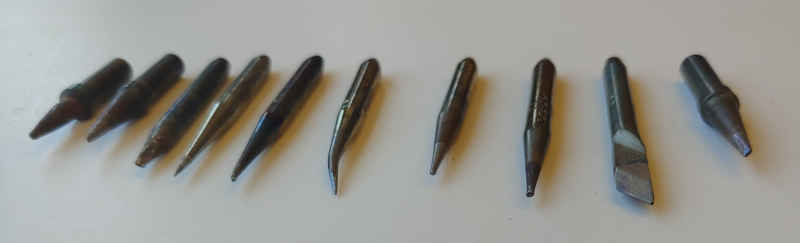
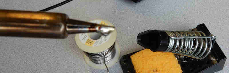
The iron tip on this image is the incorrect size for applications on the circuit board since it is too wide. It may overheat the solder joint and the area of the circuit board that is close to the solder joint. Also, this shape and size of the iron tip are inappropriate for soldering small electronic components especially surface-mount components.
The two tips shown in this image can be used for the great majority of soldering projects on the circuit boards.
On the left side is the conical tip 1/32” (0.8 mm) which is an excellent tip for soldering and desoldering fine through-hole components including integrated circuits (IC) and most surface mount devices (SMD).
The chisel tip 3/32” (2.38 mm) to the right is good for larger soldering junctions such as soldering wires, connectors, terminals and large components onto circuit boards. It is also good for tinning of wires or larger ground areas on circuit boards.
Type of circuit board
Before you start soldering components on a circuit board you must first know what kind of board you are dealing with. Circuit boards are ranging from simple single-sided circuit boards to multi-layered boards.
If electronic components are soldered on only one side of a circuit board, it is a single-sided board. The single-sided circuit board has a serious limitation when you have multiple interconnections between components. The connecting line between components on the circuit board should never cross another connecting line.
The easy solution to this limitation is to add another layer of copper on the other side of the board what leads to a double-sided board. This greatly increases the number of possible paths that conductors can be routed along.
So, if electronic components are soldered on both sides of a circuit board, it is a double-sided board. The electronic components are mounted on the top side of the circuit board. Leads of the component are run through metalized holes (also known as plated through-holes) and soldered on the other side of the circuit board. The solder should flow through the entire hole providing electrical connection on both sides of the metalized hole.
A multi-layered board has three or more layers. Additional layers are inserted between the top component side layer and the bottom side layer of a circuit board.
Each type of printed circuit board must be approached differently when soldering electronic components on them.
Cleaning
For proper soldering to occur, thorough cleaning of the surfaces must be done.
Cleaning may be done with a brush or cotton swab. For stubborn stains use isopropyl alcohol or other cleaners.
Avoid touching surfaces of solder joint with fingers since the oil on fingers is a contaminant. If you for any reason need to touch then clean them again after touching.
If the surfaces were not cleaned, the connection may look like a ball that sits on the copper pad. That is a poor junction that does not provide electrical connection nor mechanical support.
Solder
Solder is a mixture of tin and lead. The most common types of solder are 60/40 (60% tin and 40% lead) and 63/37 (63% tin and 37% lead). Solder is the filler material in solder junction.
When tin and lead are mixed together, the melting temperature of the alloy is lower than the melting temperature of either tin or lead.
Melting temperature is the point at which the solder goes from a solid-state to a liquid state. For 60/40 solder the melting temperature is 370 °F (188 °C).
Because of its low melting temperature, the solder melts quickly and, therefore, exposes the component to heat for the shortest possible time.
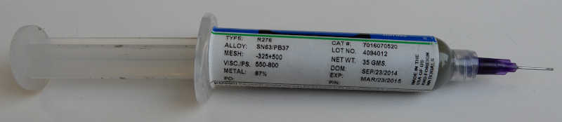
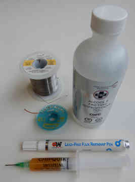
The solder used for soldering circuit boards comes in two forms: solder wire and solder paste.
The solder wire is coiled onto a spool. The sizes of solder wire used in electronics are between 0.010”-0.050” (0.25mm -1.27 mm).
Solder paste has a relatively short shelf time. The shelf time of solder paste is in the range of 3-6 months. If you wish to extend the shelf time of solder paste, it must be refrigerated.
Solder paste must be stored in a sealed container. If the solder paste container is left open, that will cause the solder to oxidize
The latest trend is to remove lead from solder because it has been listed as a hazardous material. Attempts are made to replace it with another metal such as silver and bismuth. However, this new alloy has a higher melting temperature and when in a liquid state it doesn’t flow smoothly as tin/lead alloy.
New tin/silver alloy is more environmentally friendly but it doesn’t make as good a joint connection as tin/lead solder.
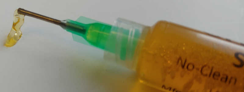
Flux
The flux is used to remove oxides from the surfaces to be soldered and to prevent new oxides from forming during the soldering process.
Rosin flux is the most popular type of flux for applications in electronics. It is made from the extract of pine sap.
The majority of solder wires contain a flux in their core. If you need one piece of solder wire from the spool, you should cut it with wire cutters. Do not tear or pull solder wire off a spool. There is a precise amount of rosin flux in the center of the wire. When you tear the solder wire to separate from the spool you change the solder/flux ratio.
Flux is available separately in form of pen or paste.
If needed, additional flux can be applied to the solder joint and leg or pin of the component.
Flux must have an activation temperature lower than the melting point of the solder. Flux usually activates at a far lower temperature than solder. If the flux is not activated during soldering it is an indicator of the bad solder joint (very likely it is an indicator of a cold solder joint).
Soldering
Finally, we are ready to start soldering.
Turn on your soldering with the proper iron tip already installed. Let the soldering iron heat up. The majority of soldering irons can reach working temperature in less than a minute.
Tinning
The iron tip should be tinned before soldering. Tinning is the process of covering the metal surface with a thin layer of solder. A soldering tip can last much longer if it is regularly and properly tinned and cleaned.
When iron reaches working temperature apply solder to the tip. The iron tip must be hot enough when doing tinning. It is better to use a thicker solder wire with a diameter of approximately 0.050” (1.27 mm) Melt a couple of inches of solder. The solder that drips off the tip will take many of the oxides and other contaminants away.
If the iron tip is not used for a longer time and has a thick oxide layer, a proper cleaning of the tip should be done before tinning. For this, you may use a brass wire tip cleaner. Insert the iron tip into the brass wire tip cleaner and twist it a few times.
Never use a steel brush instead of brass wire tip cleaner to clean the iron tip since it will damage the plating on the tip.
An iron tip should be tinned after each use as well. A little amount of solder needed for tinning can extend the life of your iron tip and save you the costs of replacing a tip.
Surfaces to be soldered should be tinned as well. It improves solderability and prevents oxidation of the surfaces during the soldering operation.
You should start tinning only on the clean and undamaged surface.
Tinning must be done prior to connecting the surfaces. After tinning, the surfaces should be shiny.
Soldering
Soldering is the process of joining two metals to make an electrical and mechanically strong connection.
When soldering through-hole electronic component to a circuit board, component’s leads are bent to fit through the board, inserted flush against the board’s top surface.
Components that become hot when the circuit board operates (such as high power resistors) are raised above the surface of a circuit board for better air circulation.
Then leads are spread outwards so that the component grips the board. Don’t bend component's leads more than 45° .
For passive components such as resistors and capacitors, is better to cut the surplus wire leads off first to have better access to the joint.
The circuit board is turned over, all leads of a component are soldered and surplus wires leads are cut off
On the other hand, for semiconductors such as transistors and diodes, it is better to do solder it first and then to cut the extra length of wire leads off.
The surplus wire leads take some of the heat from the soldering joint and prevent heat damage to semiconductor components during soldering.
It is a good technique to hold a lead of a temperature-sensitive component with metal tweezers.
If you grab the lead between the solder joint and the body of the component them the tweezers will take the excess heat and therefore protect components from heat damage.
An integrated circuit can be soldered directly to a circuit board, but it is better to solder pins of dual-in-line (DIP) socket to a circuit board and then put the integrated circuit into the socket.
That way the integrated circuit is prevented from heat damage during soldering. It is also much easier to replace an integrated circuit that is plugged in the socket than one in which pins are soldered directly to a circuit board.
Removing flux residues
After soldering, all flux residues must be removed to prevent possible degradation of the PCB.
If the flux residues are left on the PCB they can cause a change in board resistance which leads to inaccurate test results.
Flux residues can also cause changes in circuit performance once the PCB is connected to power and starts to operate in an electronic device.
Removal of flux residues can be done in two steps: cleaning and rinsing.
The best way to clean flux residue is with isopropyl alcohol.
Flux residues can also be removed with a flux remover pen.
After you remove flux residues with alcohol, then in the second step rinse the solder joint with distilled water, not tap water. Tap water may leave stains on the PCBs since it contains minerals.
Inspection
After soldering, inspect the solder joints for any defects such as a cold solder joint, bridging, solder ball etc. If you notice any defects, fix them immediately. The majority of bad solder joints could be easily repaired by re-soldering them.
When soldering joints on the circuit board look bad they very likely are bad. However, the good external appearance of the soldering joint can often be misleading. While soldering an electronic component to the circuit board the person can damage the component or circuit board in a way that is not visible. The electronic circuit can still work for a while but its operation life and reliability can be significantly reduced. Visual inspection may not reveal what is underneath.
Circuit boards
A circuit board is a platform for mounting and interconnecting electronic components. The use of circuit boards in commercial devices has started in the 1950s.
Circuit boards can have low-density packing or high-density packing.
On low-density circuit boards, the electronic components are widely spaced apart while on high-density circuit boards the electronic components are soldered very close to each other with a little space in between them.
Obviously, it is much easier to solder, assemble or repair the low-density circuit boards.
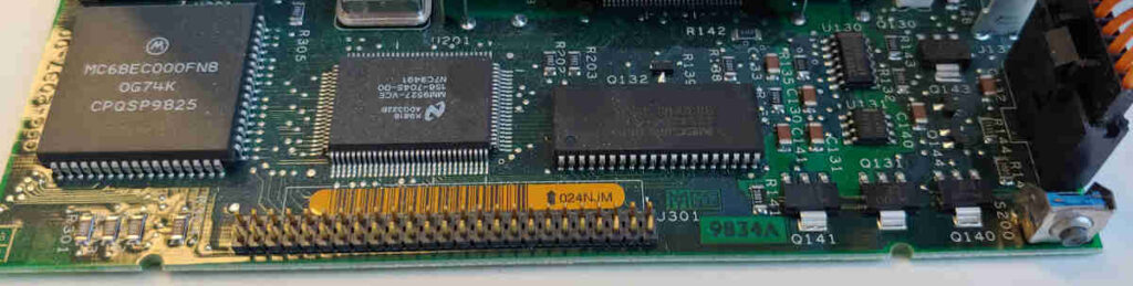
High-density circuit boards are usually populated with surface-mount components. All electronic components on a high-density board may be mounted so close together that sometimes it may not possible to rich particular components with soldering iron.
It is impossible to solder or de-solder a component if a gap between components on a board is smaller than the size of the iron tip.
For high-density circuit boards, we should use a tiny conical tip in size 3/64 inches (1.2 mm) or smaller.
When repairing a circuit board, a repair person is required to replace a damaged electronic component with a new one and restore the circuit board to its original performance. During component removal, the repair person should pay attention not to make any damages to traces or pads on the circuit board. Too much heat can burn or crack small traces on the circuit board.
Circuit boards can be uncoated or coated with a variety of coating materials.
Circuit boards consist of two main parts: base material or substrate and circuitry made of conductive copper foil which is bonded to the base material.
The base material is non-conductive. The majority of current circuit boards in electronics use FR4 glass-reinforced epoxy laminate material as a substrate. FR4 is green in appearance.
The base material must have high insulation resistance, good temperature stability and low moisture absorption. The most common thickness of printed circuit boards is 0.031” (0.787 mm) and 0.060” (1.5 mm).
The second main part of a circuit board is a thin conductive copper foil.
It consists of the conductors, pads and terminals
These copper conductors and pads are often plated with a thin layer of solder to reduce corrosion.
It also makes it easier to solder electronic components to such surfaces since the surface is already pre-tinned. .
The circuit board may be coated with a layer of epoxy which gives it a green appearance.
A silk mask can be added to the circuit board to help assemblers with component placement and orientation.
The most common thicknesses of the foil are half-ounce copper, one-ounce copper and two-ounce copper.
These units indicate the weight of copper per square foot. For example, a half-ounce board has a half ounce of copper per square foot. The more copper, the ticker copper foil is, and, therefore, the board can conduct the higher current.
A circuit board usually has several holes drilled through it to allow the mounting of electronic components.
Plated-through holes have their wall coated with solder running through the board from one side to the other.
That way, plated-through holes form a conductive path from one side of the circuit board to the other.
Electronic components
Electronic components on circuit boards may be found in a variety of sizes and shapes from standard through-hole electronic components and miniature surface-mount components to multi-leaded integrated circuits.
The leads of electronic components may be of various spacing and dimensions.
Tools
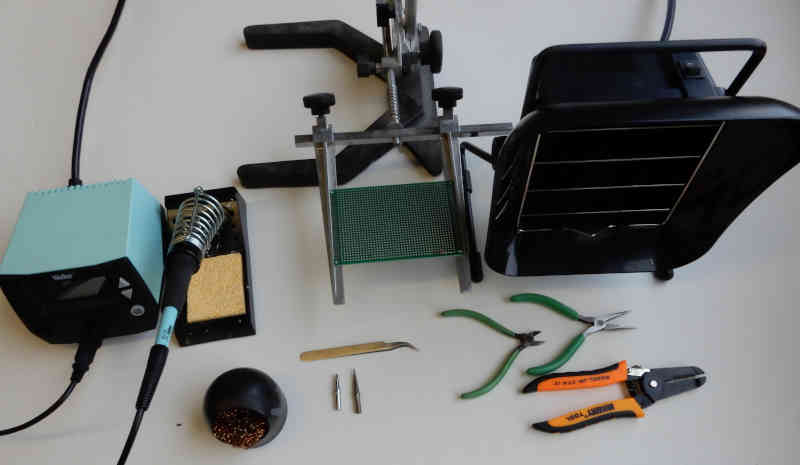
The following tools were used in this “How to solder circuit boards” guide:
temperature-controlled soldering iron WE1010 Weller (including a base station, a stand for iron and sponge)
solder tips ET series - the conical tip 1/32” (0.8 mm) and the screwdriver tip 3/32” (2.38 mm)
fume absorber Weller WSA350
round nose pliers
wire cutters
wire strippers
circuit board holder
tweezers
cleaning brushes
brass wire tip cleaner
The following accessories were used in this “How to solder circuit boards” guide: